uLED Mass Transfer Carrier and Packaging Solutions
Optimized for Next-Generation Display
Technologies
Chunyang Technology offers a range of high-performance carriers for micro and mini LED mass transfer applications. From chip transfer, bonding, rework to precision alignment, our carrier platform meets the demanding requirements of high speed, high accuracy, and high yield in modern display manufacturing.
COC Plus Donor & Donated Carrier|Dual-Function Laser Transfer Platform
Key Features:
• Functions as both COC1 Donor and Donated carrier in a single
configuration
• Utilizes laser-induced pressure wave for efficient chip transfer;
supports repeated chip placement at the same location
• Ideal for high-precision laser transfer processes with full
automation and high-yield demands
Application
Scenarios:
• COC1-phase laser transfer for uLED manufacturing
• Microchip rework and repeat chip placement

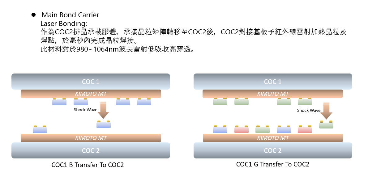
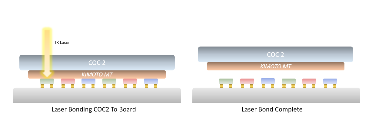
Main Bond Carrier (Laser & Stamp)|Laser & Stamp
Bonding Platform
Key Features:
• Supports laser bonding at 980–1064nm wavelengths with low
absorption and high transmittance
• Compatible with infrared laser heating, enabling millisecond-scale
bonding
• Also supports stamp bonding with excellent thermal conductivity,
heat resistance, and tack stability — enhancing yield and minimizing sheet loss
Application
Scenarios:
• COC2-phase bonding process for uLED
• Dual-process platforms combining laser and planar hot press bonding
Stamp Bonding Donor Carrier|High-Stability
Alignment Carrier
Key Features:
• Delivers consistent tack value, ensuring precise chip alignment
without displacement or skew
• Suitable for thermal transfer processes in high-precision stamp
bonding
Application Scenarios:
• Stamp bonding during the COC2 phase
• Applications requiring high alignment accuracy using stamp
compression

Repair Donor Film|For Precision Rework
Processes
Key Features:
• Dedicated for COC2-phase rework; supports chip alignment and
transfer to blue tape or stamp platforms
• Enables accurate chip repositioning and rework, enhancing yield
control and material utilization
Application Scenarios:
• Post-transfer rework for COC2 uLED chips
• Precision chip replacement or selective reworking operations

B-stage Sheet Encapsulation Film|For micro/Mini LED & Semiconductor Packaging
Key Features:
High-reliability encapsulation solution
designed to enhance transfer accuracy and process stability.
Application Scenarios:
Chunyang provides B-stage thermosetting
encapsulation films engineered for micro/Mini LED mass transfer and advanced
semiconductor packaging. These pre-cured films feature controlled flowability,
adhesion stability, heat resistance, and low residue, making them ideal for
multi-layer stacking, chip attach, and wafer-level packaging (WLP). The films
help improve alignment accuracy and process consistency while reducing yield
loss.
 Focused expertise in uLED process materialsEnd-to-end solutions covering transfer, bonding,
rework and packaging.Full technical support, fast sampling, and quick
turnaround
Contact us today for a free sample or technical
white paper!